.png?ext=.png)
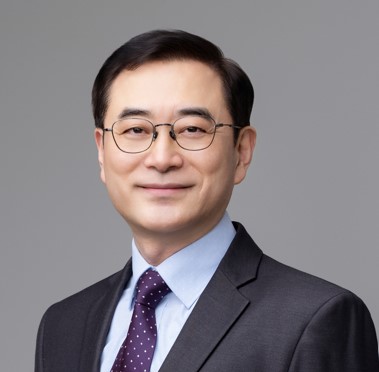
Changwook Han is a renowned expert in the display field with over 35 years of experience. He serves as the Principal Analyst and Executive Vice President in charge of the entire research team at UBI Research. He provides industry-leading insights accumulated through years of experience and a global network. His areas of interest include the market, technology, and industry dynamics of OLED and micro-LED products, and automotive displays. Prior to joining UBI Research, he served as a vice president and head of OLED device development at LG Display, where he led the development of next-generation OLED, EL-QD, micro display and other devices. He also served as a team leader for LCD development and OLED TV device development at LG Display, gaining experience in the mass production of OLED and LCD products, including the world’s first large-size OLED TV and transparent OLED display. He received his bachelor's and master's degrees in Inorganic Materials Engineering and his Ph.D. in Electrical Engineering from Seoul National University in Seoul, South Korea. He is also an adjunct professor in the Department of Chemistry at Korea University, teaching display subjects.
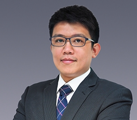

With over 20 years of experience in the display industry, I have conducted
extensive and in-depth research on technologies such as LCD, OLED, Micro
LED, and NED.
Offering analysis on the industry development from various perspectives
with his people's connection in the segment and professional knowledge
regarding sales, technology, and supply chain management.
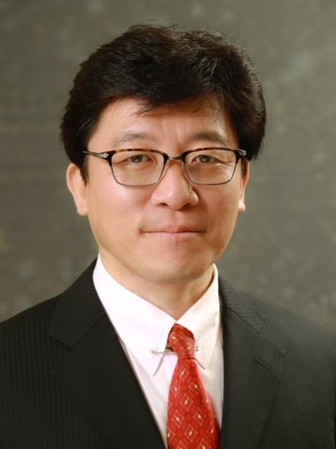

Yoshio Tamura joined Counterpoint Research as part of its acquisition of DSCC, where he was Co-Founder and President of Asian Operations at DSCC, based in Tokyo, Japan.
He is a more than 30-year veteran of display market research and consulting and is one of the foremost authorities on the display market and its supply chain. He started covering this market in 1990 at Techno Systems Research (TSR) where he launched their display market research business and grew it rapidly. After 10 years at TSR, in 2000: he was invited to join DisplaySearch, as Vice President and representative for Asia and Japan, and he was the first employee of DisplaySearch Asia. After that, through his personal connections, DisplaySearch expanded its base to other Asian countries than Japan by hiring a lot of human resources in Korea, Taiwan and China. In 2005: DisplaySearch grew into the world's most prominent display research and consulting company in just five years and is acquired by NPD in USA. He became Senior Vice President and Fellow in NPD's DisplaySearch division. In 2014: NPD's DisplaySearch business unit, which has grown even larger, is acquired by IHS in UK. He became Senior Director of IHS's display business unit. In 2016: He left IHS in August and began operations in October as co-founder and President of Asia for Display Supply Chain Consultants (DSCC) in USA. In August 2023: DSCC that has grown over the past seven years since its establishment, is acquired by Counterpoint Research.
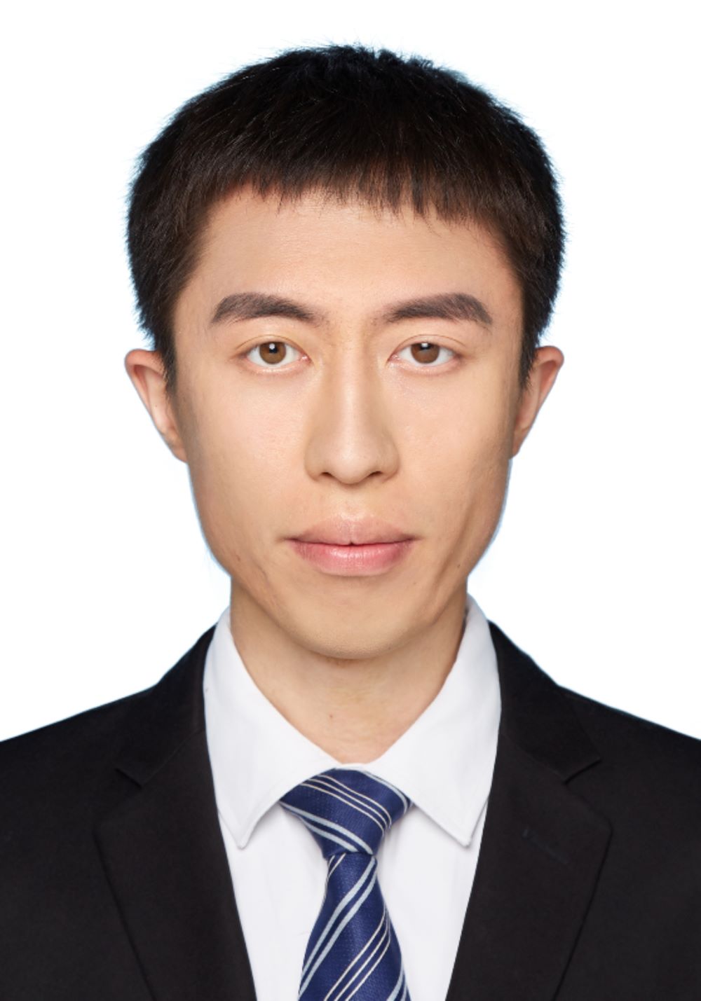

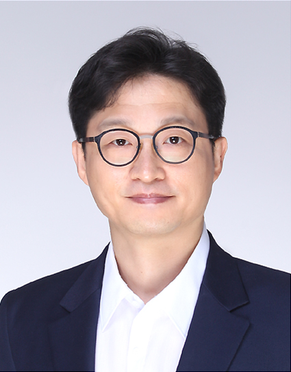
I received my PhD in Materials Science and Engineering from the Department of Chemical Engineering at Tsinghua University in 2019. Afterwards, I joined BOE and worked as a senior researcher at the Central Research Institute up to now. I am working on QLED electroluminescence (EL) technology for the display application, and focusing on the optimization of QLED device efficiency and large-area process manufacturing. I have published several articles and patents in this field.
.png?ext=.png)
Yeo-Geon Yoon received B.S., M.S and Ph.D in material science and engineering from Seoul National University, Korea.
After receiving Ph. D in 2004, he joined Samsung Display and he has researched on the process engineearing of TFTs , printing and QD
for display application as a leader of Process Research Team in Samsung Display Co., Ltd.


Hunter McDaniel, PhD is UbiQD’s Founder and CEO. He transitioned from a postdoc position at Los Alamos National Laboratory to the company’s first full-time employee in 2014. His vision for the company is to become the worldwide leader in quantum dot manufacturing by enabling new products that aren’t possible with toxic CdSe or InP QDs. He has extensive relevant technical experience as he has worked on both traditional II-VI QDs (including those that contain cadmium) and I-III-VI QDs. During his career, Dr. McDaniel conducted research at top-tier research institutions; Los Alamos National Laboratory (postdoc 2011-2014), Argonne National Laboratory (2011), University of Illinois at Urbana Champaign (PhD 2006-2011), and University of California at Santa Barbara (BS 2001-2006)). He is highly experienced in the materials science of semiconductor nanocrystals and their optoelectronic device applications (e.g., solar cells, LEDs) with over twenty research publications and more than 700 citations.
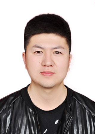

Dr. Rongzhen Cui is a Senior Researcher in Organic Light-Emitting Materials at Visionox Technology Inc. His work focuses on the development of novel high-efficiency organic light-emitting devices (OLEDs) for full-color displays, employing advanced mechanisms such as triplet-triplet annihilation (TTA), hyperfluorescence, and quantum dot (QD) photoluminescence (PL). At this conference, he will share his insights on photolithographic-patterned QD-OLED technology.
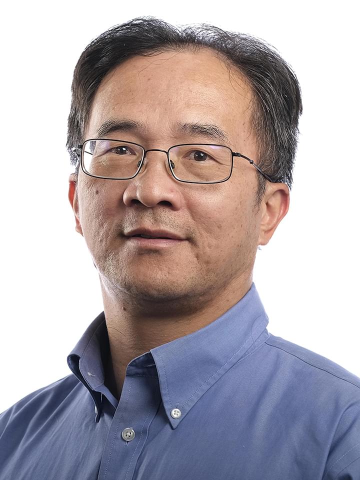

As the world leading marketer and application expert in quantum dot (QD) technology for display, Dr. ZhongSheng Luo has extensive experience in commercializing Quantum Dot Enhancement Film (QDEF) and deep involvement in the development of new QD applications for display such as QD-microLED, QD-OLED and electroluminescent NanoLED. He is the VP&GM, Application Development, Products and Revenue of Nanosys. He obtained his Bachelor's and Master’s degrees in Materials Science and Engineering from Tsinghua University, China and his Ph.D in Materials Science and
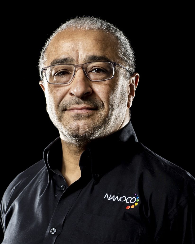

Nigel Pickett co-founded Nanoco Technologies and is the inventor of Nanoco’s key quantum dot scale-up technology. He is a versatile senior executive with materials, chemistry and processing expertise, combining strategic commercial and technical skills with a 25-year track record of translating complex technical challenges into commercial solutions. He has a passion and experience in taking research work from the academic bench through to full commercialisation.


Dr. Igor Nakonechnyi is the co-founder of QustomDot, a company he helped launch in 2020. His deep expertise in colloidal quantum dots (QDs), cultivated since his postdoctoral research at Ghent University (following a PhD equivalent in solid-state chemistry from Chernivtsi National University in 2013), powerfully informs QustomDot's product development strategy, with a significant focus on innovative ink-jet inks for Quantum Dot Color Conversion (QDCC) in next-generation displays. Igor also leads efforts in securing government funding, managing partnerships, fostering agile R&D, building a talented technical team, and overseeing intellectual property as a member of the board of directors. His work is dedicated to advancing QD applications and large-scale production while ensuring their stability, particularly within the rapidly evolving display technology sector.
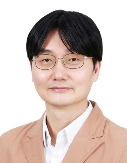

Tae-Woo Lee is a professor in the Department of Materials Science and Engineering at Seoul National University, Korea. He received his Ph.D. in Chemical Engineering from Korea Advanced Institute of Science and Technology (KAIST), Korea, in 2002. He joined Bell Laboratories, Lucent Technologies, USA, as a postdoctoral researcher in 2002 and then worked at Samsung Advanced Institute of Technology as a member of the research staff (2003–2008). He was an assistant and associate professor in the Department of Materials Science and Engineering at Pohang University of Science and Technology (POSTECH), Korea, until August 2016. He received numerous prestigious awards, including the Merck Award (2006), Korea Young Scientist Award from Korea President (2008), the Scientist of the Month Award from the ministry of science, ICT and future planning in Korea (2013), Research Innovation Award from Ministry of Science and ICT of Korea (2018), Korean Engineering Award (Presidential Award) (2021), Commendation from the Ministry of Trade, Industry and Energy of Korea (Minister’s Award) (2021), and Kyung-Ahm Prize (2023). He was appointed as a Fellow of Korea Academy of Science and Technology in 2021. He was honored as 2020 MRS Fellow and 2024 SPIE Fellow.
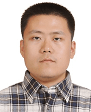
Longjia Wu received his Bachelor degree in Materials Science and Engineering from Wuhan University of Technology (WUT), and then got his Ph.D. degree in Materials Science and Engineering from University of California, Davis (UC Davis) in 2015. After graduation, he joined TCL Corporate Research, engaging in the development of high performance quantum-dot light-emitting diodes for display application.
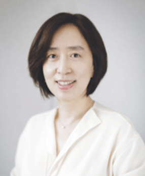
Sohee Jeong is a Professor in the Department of Energy Science at Sungkyunkwan University (SKKU). She received her BS and MS degrees in Chemistry from KAIST and earned her PhD in Chemistry from the University of Michigan. She conducted her graduate and postdoctoral research in the Quantum Dot Group at Los Alamos National Laborator. She later held positions as a Senior and Principal Researcher at the Korea Institute of Machinery and Materials (KIMM). In 2010, she further broadened her research scope as a visiting scholar at the National Renewable Energy Laboratory (NREL), where she investigated quantum dot solar cells. Dr. Jeong's research focuses on the surface chemistry of nanocrystal quantum dots, particularly the fundamental mechanisms that govern charge transfer and key optoelectronic properties. Her work contributes to advancing the science and technology of quantum-confined nanomaterials for applications in electronics, photonics, and energy conversion. She is also active on editorial boards. (e.g. Chemistry of Materials)

Andras Pattantyus-Abraham has been working on commercializing quantum-dot based image sensors since 2013, when he joined Invisage Technologies to work on RGB and NIR imaging. He joined Apple in 2017, where he became Senior Manager of QD R&D. In 2020, he transitioned to STMicroelectronics and became Director of Advanced Materials R&D for QD sensors, now focused on SWIR sensing and imaging. In October 2024, he founded BestQD Solutions LLC to help accelerate the adoption of low-cost QD-based SWIR imagers. He has deep expertise in QD synthesis, quality control and QD-based optoelectronics design, processing, testing and application development.
He has B.Sc.’s in Engineering Physics and Mathematics from Queen’s University and a Ph.D. in Chemistry from the University of British Columbia. He also worked as a postdoc and principal scientist under Ted Sargent at the University of Toronto, where he did pioneering work on depleted heterojunction QD photovoltaics.

.png?ext=.png)
Tobias Halouzka is a Junior Chemist at QDI Systems, where he specialises in the synthesis and analysis of quantum dot solutions. He holds a Master's degree from the University of Groningen and has a background in Materials Chemistry and materials characterisation. His work focuses on developing scalable quantum dots for shortwave infrared absorption.


Markus Suta studied Chemistry (MSc) at the University of Siegen, Germany, and obtained his PhD degree in Chemistry in the group of Claudia Wickleder in 2017. He followed up with a second degree in Physics (MSc) with specialization in Theoretical Physics in the group of Thomas Mannel in Siegen. From 2018 to 2021, he has been working as a postdoctoral researcher in the group of Andries Meijerink at Utrecht University, The Netherlands. Since 2021, he has been holding a tenure track position for Inorganic Photoactive Materials at the Heinrich Heine University Düsseldorf, Germany. His interests lie in the development and a fundamental understanding of new inorganic phosphors for various applications such as LEDs, luminescent thermometry, upconversion, as well as a better understanding of nonradiative transitions. For that purpose, he and his group combine inorganic synthesis and structural chemistry in solid-state systems with advanced optical characterization by means of luminescence spectroscopy as well as theoretical modelling.
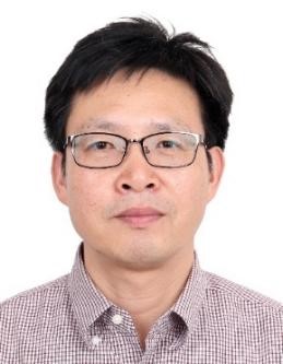
Rong-Jun Xie obtained his PhD in Inorganic Non-metallic Materials at Shanghai Institute of Ceramics, Chinese Academic of Science in 1998. After carrying out post-doctoral work at National Institute for Materials Science (NIMS, Japan), National Institute for Advanced Industrial Science and Technology (AIST, Japan), and Alexander von Humboldt (AvH) research fellow at Darmstadt University of Technology (Germany), Xie joined National Institute for Materials Science (NIMS) as a Senior Researcher in 2003, and was promoted to Principal Researcher in 2007 and to Chief Research in 2017. In 2018, he moved to Xiamen University as a full professor at College of Materials.
Xie’s research interests include (i) phosphors for lighting and displays; (ii) mechanoluminescent materials for sensing technologies; and (iii) quantum dots and emissive displays. He has contributed to 300+ published papers and 100+ invited talks, and held 50+ patents.
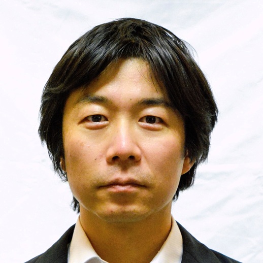
I've received my Ph.D. in Engineering in 2010 for a field of nano-scale dielectric properties near semiconductor/oxide interfaces using first principles calculations at the University of Electro-Communications, Japan. Since I joined Nichia in 2010, I've been working in the development of new inorganic phosphors. I filed a lot of patents for inorganic phosphors and their applications.
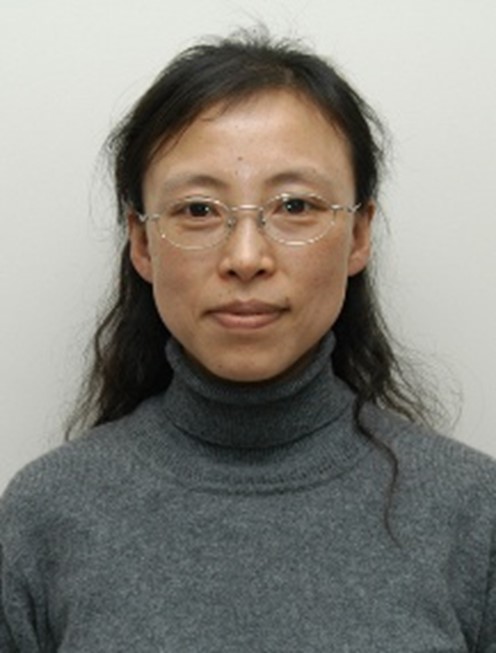
Lingdong Sun received her PhD degree in Condensed Matter Physics from Changchun Institute of Physics, Chinese Academy of Physics. Following a postdoctoral fellowship, she joined the faculty at Peking University, and was promoted to associate professor and professor. She worked as a visiting professor at Keio University and Kyoto University. Her current research focuses on the synthesis and applications of rare earth and semiconductor nanomaterials.
.jpg?ext=.jpg)

Bio coming soon......
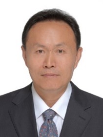
Dr. Jun Lin, professor, and the group leader of luminescent and biomedical materials in Changchun Institute of Applied Chemistry, Chinese Academy of Sciences. His research mainly focuses on luminescent materials for various applications, including photoluminescence and spectral properties of rare earth ions and peroskite QDs for applications in displays and lightening (especially for white LED), as well as multifunctional materials as theranostic agents for biomedical applications. He won Grade -1 Award for Science and Technology Progress of Jilin Province three times, and was selected in highly cited researchers in materials science and cross-field in 2014-2023. So far he has published more than 900 peer-reviewed journal articles, including Chem Rev(1), Chem Soc Rev(7), Adv Mater(25), J Am Chem Soc(7) and Angew Chem Int Ed (20) etc, with total citations over 80000 and H index of 155; He also gave more than 100 invited lectures in various kinds of conferences.